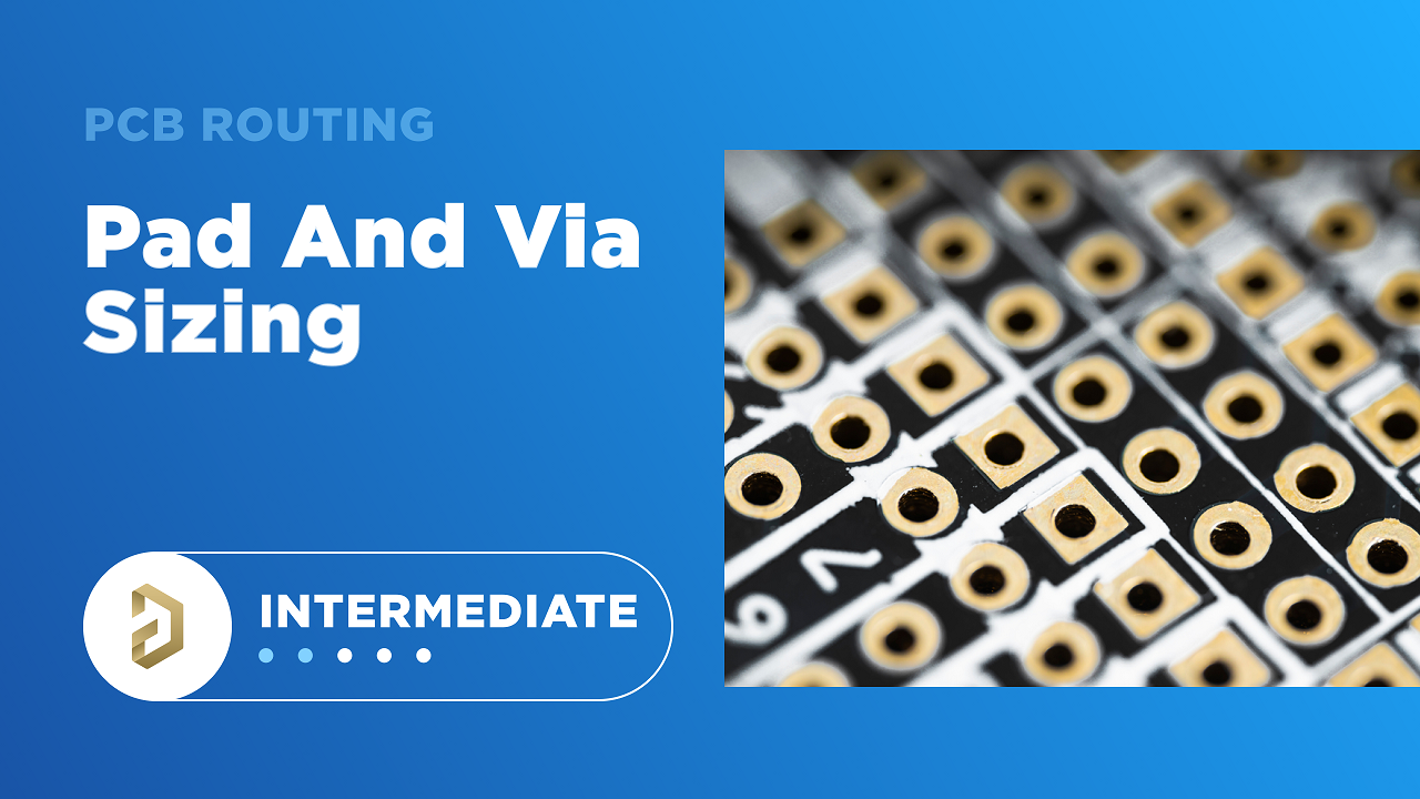
PCB Via Size and Pad Size Guidelines, Zach Peterson, Blog
By A Mystery Man Writer
Do you know what PCB via size you should use in your PCB layout? We’ll look at a few simple ways to answer this question.

Design007 Magazine :: I-Connect007

Design007 Magazine :: I-Connect007

ESR_Calculators__th.jpg

Raspberry Pi. Home automation I recently installed a GREE air

Natural sensory context drives diverse brain-wide activity during C. elegans mating

DIY Recording Equipment Blog – Page 2
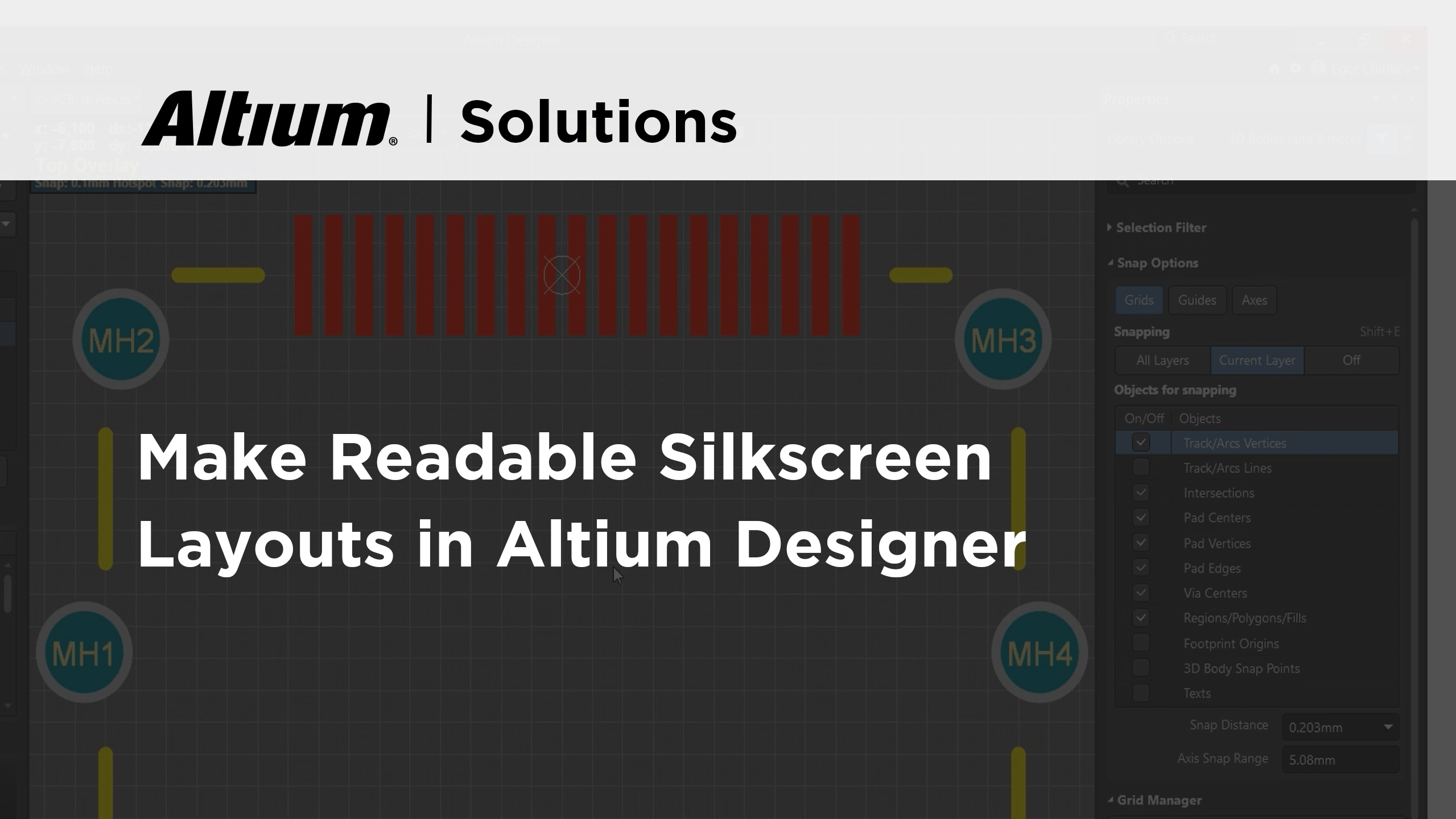
Designing and Placing Silkscreen on your PCB with Altium Designer

US9146620B2 - Input device assembly - Google Patents

B Tech Courses Ai and Ds, PDF, Corrosion

US9411751B2 - Key formation - Google Patents

US9146620B2 - Input device assembly - Google Patents

20.000 Most Frequent Words, PDF, Internet
PCB Via Size and Pad Size Guidelines, Zach Peterson

We have all been there… 😅🤚 I promise it gets better

PCB Layout Cleanup Before Manufacturing, Zach Peterson
- Always Infinity Pads with Flex Foams
- Always, Radiant With FlexFoam Pads For Women, Size 4, Overnight Absorbency With Wings, Light Clean Scent, 20 Count : : Health & Personal Care

- Always Maxi Overnight Pads - Size 4 : Target
- The Reusable Pad - 5 Piece Bundle. For Heavy Flows. – The Period Company
- Always Maxi Pads Size 4 Overnight Absorbency Scented with Wings


- DIM Women's Generous Classic Underwire x1 Bra, White, 32B : : Fashion

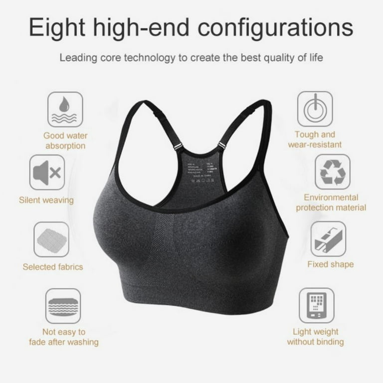
- Racerback Sports Bra for Women Seamless High Impact Running Yoga
- Fit for Me by Fruit of the Loom Women's Plus Size Microfiber Hi-Cut Underwear, 6 Pack

- Loyalty Pet Products Black Fur Resistant Leggings

- 5 Solas Five Solas Essential T-Shirt for Sale by