The complete guide to PCB pad :types, size, spacing, repair and comparison - IBE Electronics

By A Mystery Man Writer
Soldering is one of the most important processes in PCBA processing. On printed circuit boards, electrical connections to all components are made via PCB pads. The PCB pads are a very critical part of the PCB that determines where components are soldered on the PCB.The size, shape, and position of pads in a PCB directly depend on the manufacturing quality of the board. Today we will take a look at the PCB pad in SMT soldering.
Soldering is one of the most important processes in PCBA processing. On printed circuit boards, electrical connections to all components are made via PCB pad.

Printed circuit board - Wikipedia
Via Hole Types And Their Use In PCBs

How To Repair Damaged /Missing PCB Pads INVISIBLE Fix, 45% OFF

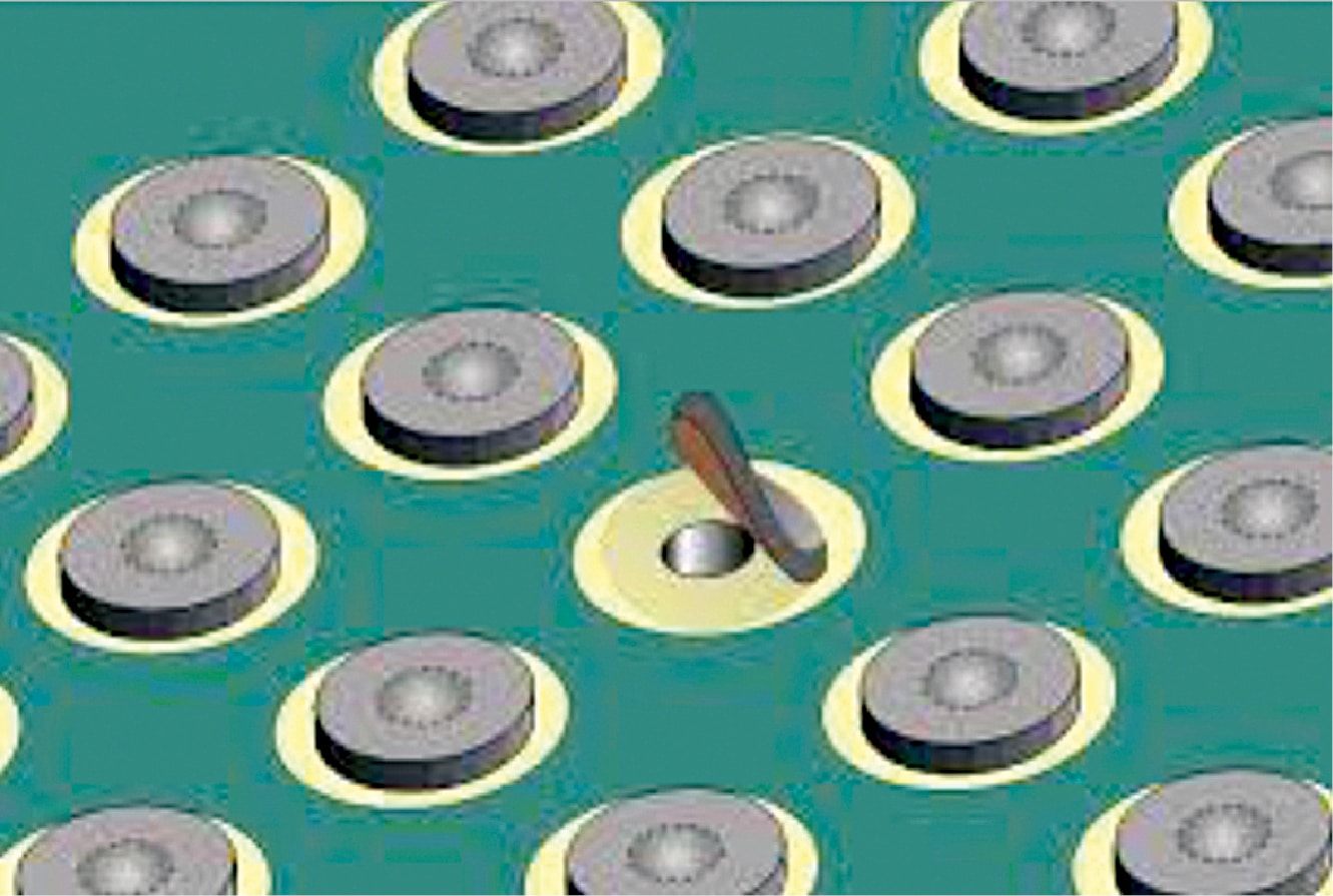
Via-in-Pad - PCB Prototype the Easy Way - PCBWay
SMT Components Size Chart: What to Know - Free Online PCB CAD Library
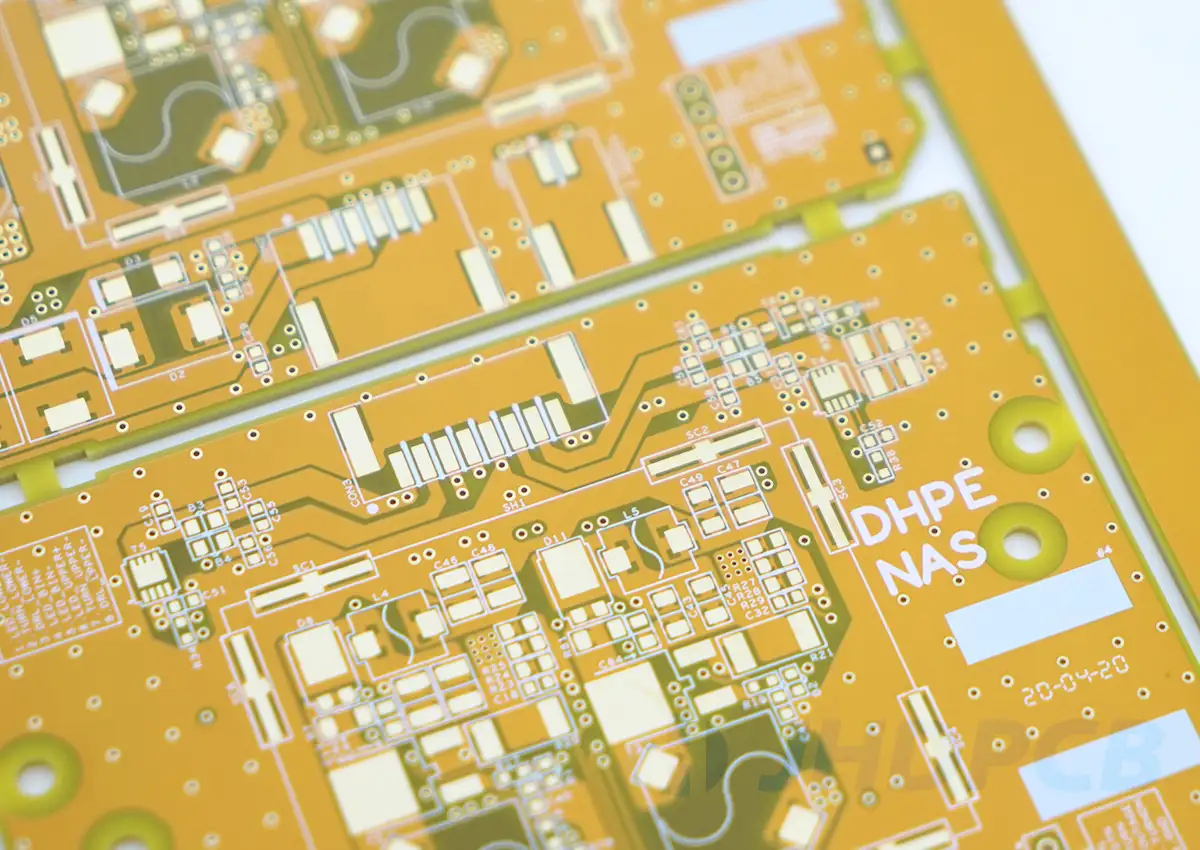
Best Guide To PCB Traces: Width, Thickness And Design Fix Recommendations - Jhdpcb
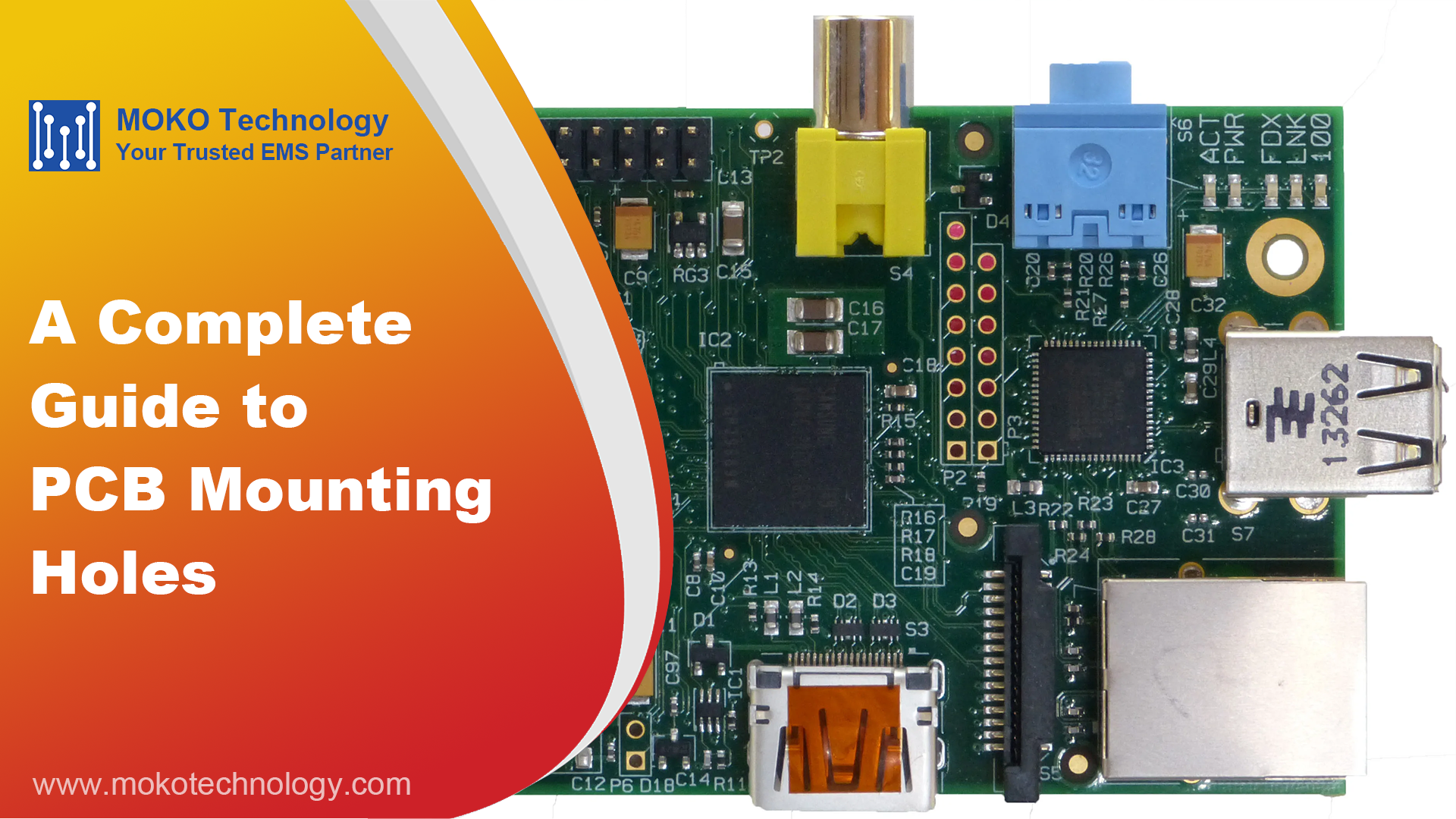
PCB Mounting Holes - What Are They? How to Design?

Solved Nep AutoZone Produces Brake Pads Using A Standard, 45% OFF

The complete guide to PCB pad :types, size, spacing, repair and comparison - IBE Electronics

How To Repair Damaged /Missing PCB Pads INVISIBLE Fix, 45% OFF
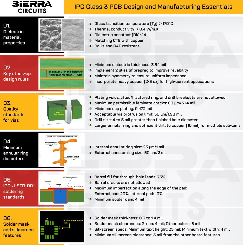
IPC Class 2 vs 3: The Different Design Rules

The complete guide to PCB pad :types, size, spacing, repair and comparison - IBE Electronics