Thursday, Sept 26 2024
What is a Pad in PCB Design and Development

By A Mystery Man Writer
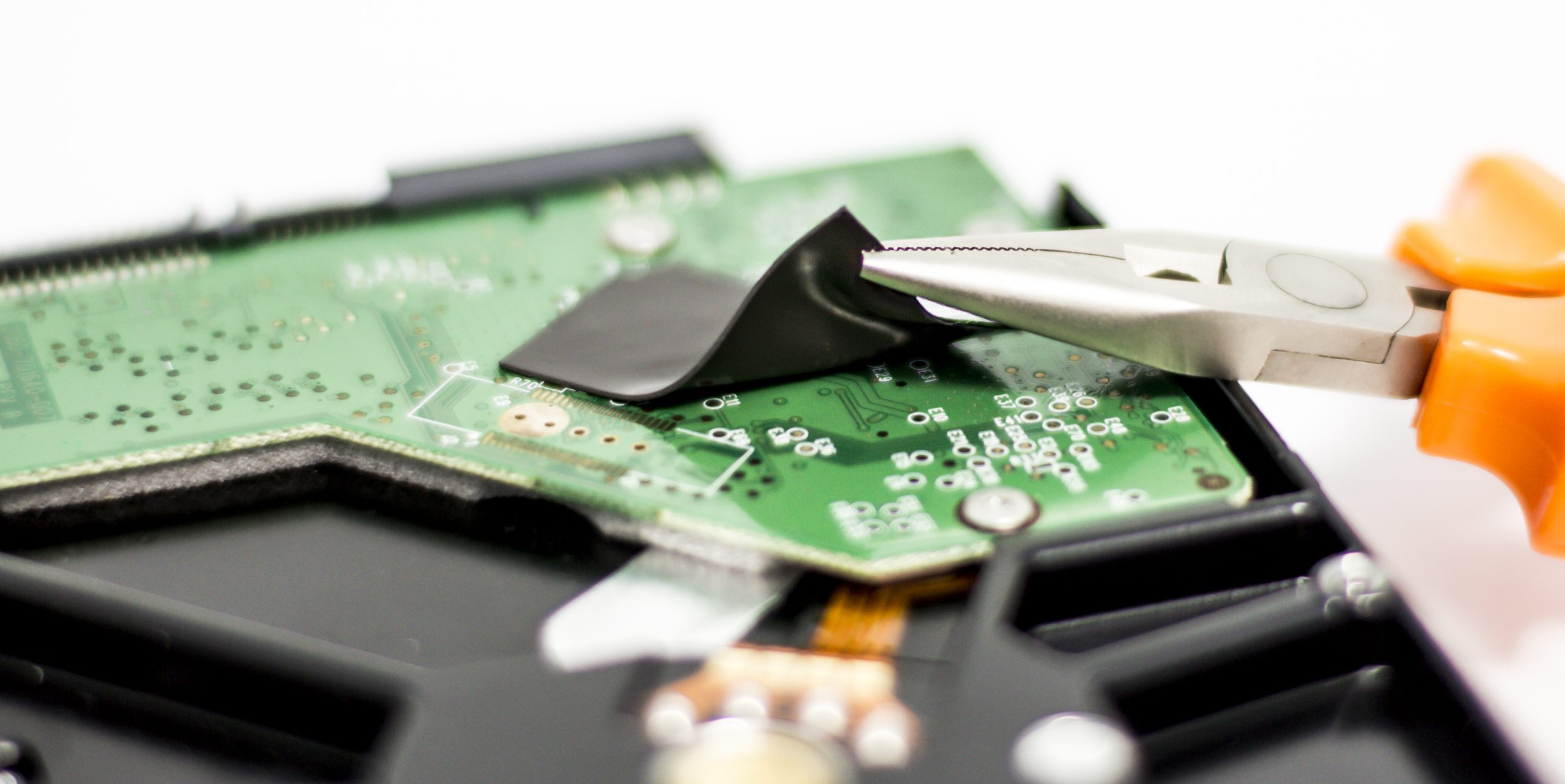
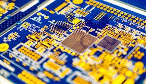
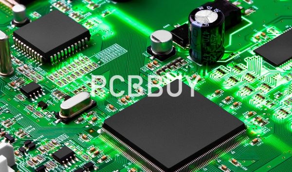
A pad is critical to PCB design as it serves as the designated surface area for electrical contact between the component and the board.
Thermal Pads in PCB Design & Manufacturing
PCB Basic Knowledge_84

How to Determine the Impedance of a Circuit - Absolute Electronics

Component Placement in PCB Design & Assembly

PCB Basic Knowledge_84
Component Placement in PCB Design & Assembly

PCB Fab Express on LinkedIn: RAPID PROTOTYPE SERVICE
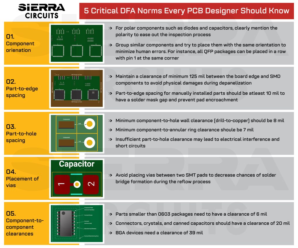
14 Tips For PCB Design For Assembly

What is a Pad in PCB Design and Development? - Absolute
PCB Basic Knowledge_84
What is DRC in PCB?
Related searches
- Mouse Pad Grande Anime One Piece 65x32 cm Setup 100 no Shoptime

- Use Drum Machine Designer pad controls in Logic Pro for Mac - Apple Support
- One Piece Logo Mouse Pad Gaming RGB Led (10 Colors) - Official One

- Women One Piece Sports Swimsuit Athletic Racerback Swimwear Pad

- One Piece Logo Mouse Pad Gaming RGB Led (10 Colors) - Official One Piece Merch Collection 2023 - One Piece Universe Store
Related searches
- The Best Snow Pants for Curvy Women - Tales of a Mountain Mama

- Boody - LYOLYTE™ - the name of our new collection is derived from us blending the benefits of our new fabric and what makes it different. ☁️ Lyo is for the
- Aerie High Waisted Crossover Rib Super Flare Legging Blue Size XS - $27 (46% Off Retail) - From Devi

- Scoop Long Sleeve Chiffon Wedding Dresses Backless Ivory Bridal Gown WD509

- Double Take 5 Pocket Capri Jeggings – Style Sifter


©2016-2024, slotxogame24hr.com, Inc. or its affiliates