Saturday, Sept 21 2024
Details of test chip designs: pad pitch, layout, materials, and opening.

By A Mystery Man Writer
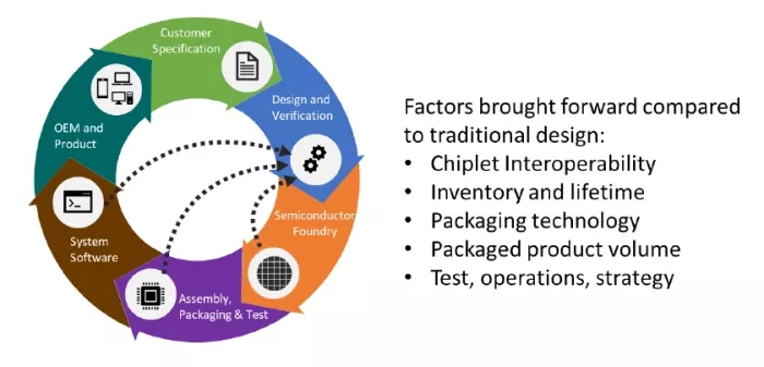
Business Analysis of Chiplet-Based Systems and Technology

Taking on the 0.3 mm ultra-fine pitch device challenge in PCB design
Sensors, Free Full-Text

AN-772: A Design and Manufacturing Guide for the Lead Frame Chip Scale Package (LFCSP)

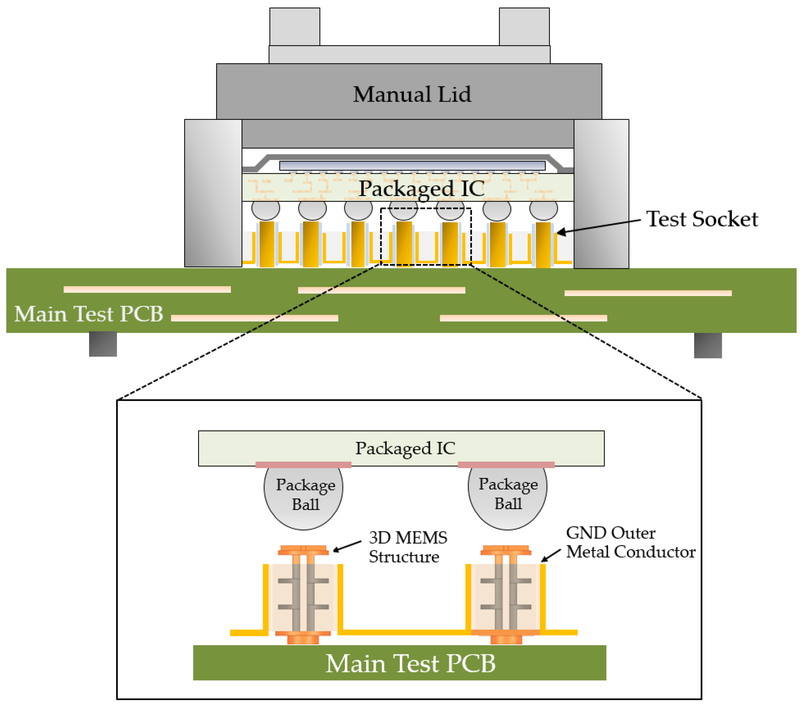
Test board layout of a single layer FR4 board (5 cm 2 7 cm) with daisy
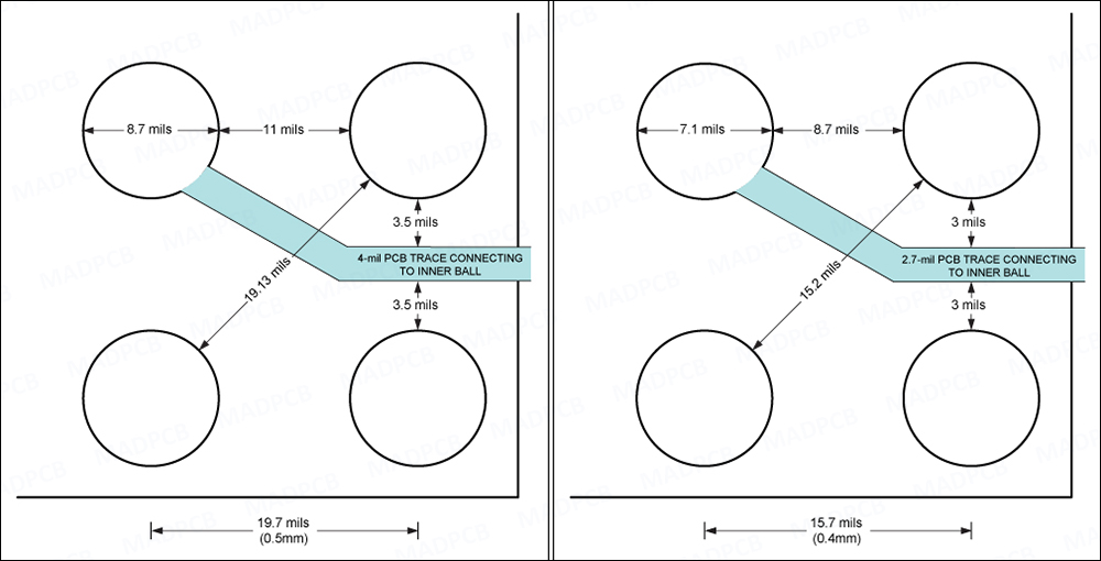
Pitch: SMD Pitch, IC Pitch - PCB Design, Fab & Assembly
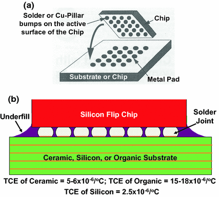
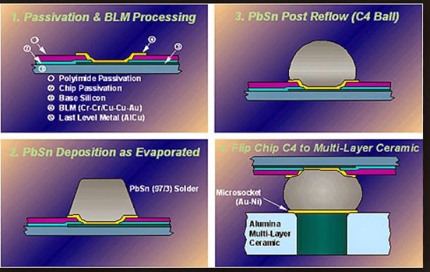
Flip Chip Technology Versus FOWLP

Integrated circuit - Wikipedia
Details of test chip designs: pad pitch, layout, materials, and opening.
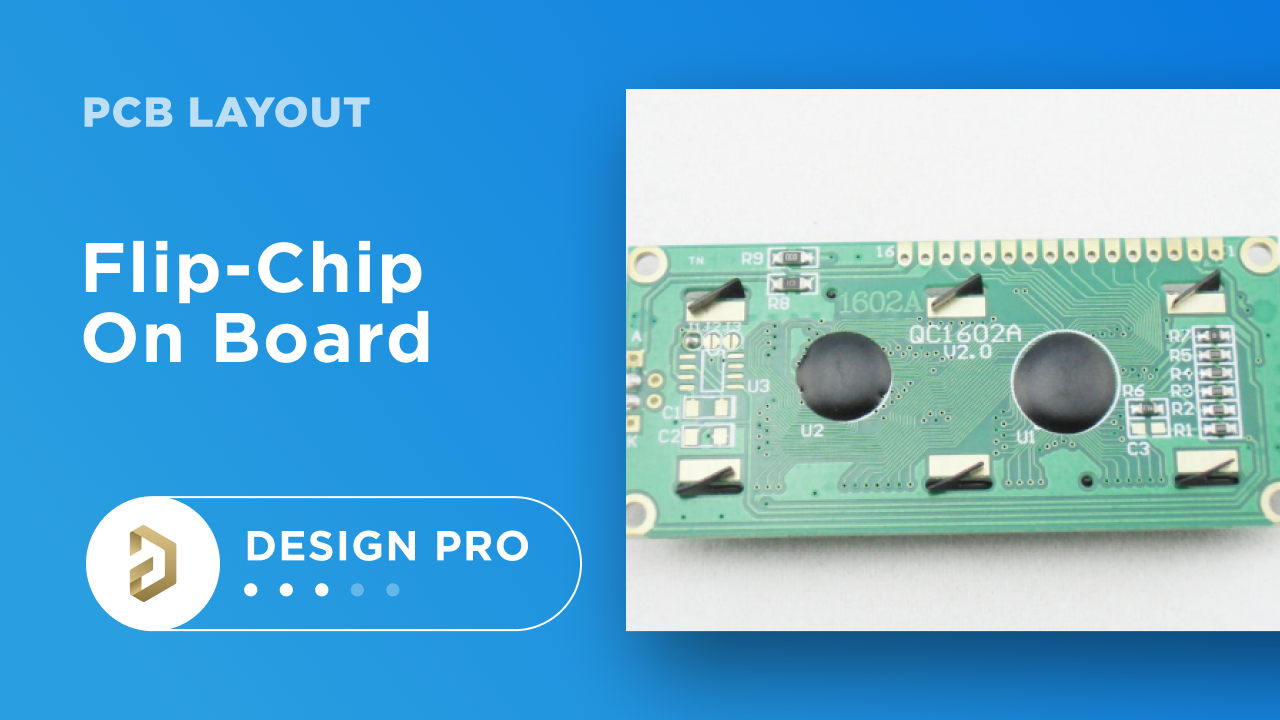
PCB Design Rules for Chip-on-Board Layout
IC I/O pad layout and choice
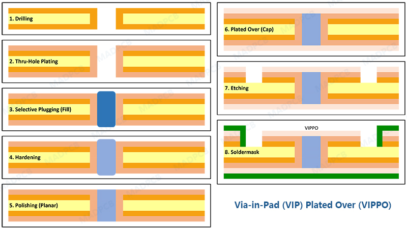
Via in Pad Manufacturing Process, PCB Manufacturer
Related searches
- Sigvaris Chip Pad Dorsum Acessórios - SIGVARIS GROUP Brasil

- Mantra VLSI : C4B controlled collapse chip connection
- Apple introduces next-generation iPad Pro, supercharged by the M2 chip - Apple (CA)
- In the iPad, Apple Is Betting on Its Own Microchip - The New York

- App note: Exposed pads on some IC packages – Dangerous Prototypes


©2016-2024, slotxogame24hr.com, Inc. or its affiliates